High-operating-temperature (HOT) IR cameras based on two new focal-plane-array technologies nBn and strained-layer superlattice (SLS)are well-suited for applications where low size, weight, and power are crucial.
ARN ADAMS and ELLIOTT RITTENBERG
Today’s fixed and mobile mission requirements are driving the development of thermal imaging systems that are smaller, lighter, and use less power, but still offer sufficiently high resolution to detect targets at long distances, thereby providing the end user with a tactical advantage. This requirement for low size, weight, and power (SWaP) sensor configurations is spurring the development of new detector technologies that promise to be less expensive to manufacture, offer increased capabilities, and operate at warmer temperatures compared to traditional IR focal-plane arrays (FPAs) that are cooled to liquid-nitrogen temperatures.
These new high-operating-temperature (HOT) detectors allow the use of smaller, long-life Stirling coolers that result in camera developments suitable for applications in which SWaP limitations are paramount. This article discusses two such detector developments nBn (two n-type semiconductors sandwiching a barrier layer) and strained-layer superlattice (SLS).
Infrared detectors today are used in a wide variety of security, surveillance, military, and commercial applications. Their ability to detect thermally emitted IR light makes them well suited for night vision, detection, tracking, search and rescue, nondestructive evaluation, gas analysis, and condition monitoring, to name just a few of the growing list of uses for this versatile technology.
Typically, infrared sensors are characteristically classified as either cryogenically cooled or uncooled. Cryogenically cooled IR cameras based on photon detectors such as indium antimonide (InSb) arrays are many times more sensitive than uncooled microbolometer-based thermal IR imagers. On the other hand, the lower cost and reduced SWaP of cameras based on uncooled thermal sensors result in systems suitable for price-sensitive applications requiring video-rate surveillance and short-focal-length optics.
Development is underway to lower both the cost and SWaP requirements of cooled thermal IR photon detectors to extend the application space where these arrays can be effectively and competitively employed. Much of this work involves HOT sensors using new semiconductor materials such as nBn and SLS, or through further development of existing materials (for example, epitaxially grown InSb).

Infrared spectral bands and applications
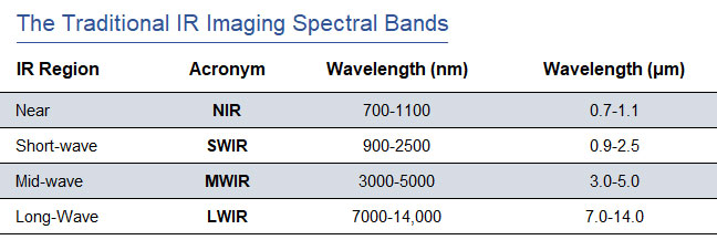
The atmosphere has several transparent regions that define the traditional IR imaging spectral bands (although spectroscopists and astronomers use somewhat different criteria). For purposes of this article, the IR imaging regions, their acronyms, and their overlapping wavelength ranges are shown in the table.
The MWIR and LWIR bands are referred to as thermal IR bands. Thermal IR refers to the wavelength spectrum from about 3 to 14 μm, where ambient-temperature objects emit copious amounts of thermal radiation.
Uncooled microbolometer arrays respond over a broad spectral range, but are optimized for the LWIR band since they require a relatively strong signal from the target of interest. The LWIR band furnishes about 100 times more photons than the MWIR band; thus, the MWIR signal is typically dwarfed by the LWIR signal for uncooled sensors.
The relatively low sensitivity of the uncooled microbolometer arrays requires fast, low f-number optics (lower than f/1.5 and typically f/1.0) for most surveillance applications. Therefore, microbolometer systems become uncompetitive in both size and cost relative to photon detectors when the lens focal length reaches about 200 mm. In addition, the relatively slow time constant of microbolometers, as well as their low sensitivity relative to semiconductor photon detectors, currently limits most microbolometers to video (~60 Hz) frame-rate applications.
The push to smaller microbolometer pixel size improves system modulation transfer function (MTF), improves microbolometer response time, and decreases cost for a given format of FPA (for example 640 × 480, 1280 × 1024, and so on), but decreases field of view for a given optic and risks an increase in system noise. It is not clear that pushing to pixel sizes less than about 10 μm makes sense for most current-technology microbolometers and applications. Look for microbolometer array manufacturing costs to drop below $100 in the next few years, pushing the technology into the consumer application space.
nBn sensors
The increased sensitivity of thermal IR photon detectors makes for a much broader range of capabilities relative to microbolometers. Cameras equipped with these sensors would be preferred for use in a wide variety of demanding applications if only the cost of the sensor arrays and resulting SWaP requirements could be reduced. For example, an MWIR nBn sensor array, first commercially developed by nBn patent holder Lockheed Martin Santa Barbara Focalplane, operates at 145 to 175 K temperatures, dependent on dark current requirements. The nBn sensor design is self-passivating, decreasing leakage current and associated noise while improving reliability and manufacturability. Because its structure limits dark current within the junction, the temperature at which it operates can be increased.
In 2011, Santa Barbara Focalplane (Goleta, CA) patented a new type of nBn detector. In principle, the extended-wavelength digital alloy nBn detector allows the cutoff wavelength to be extended to about 14 μm, though technical challenges remain for implementation at the longest wavelengths. This sensor is produced by layering strained absorber layers with very thin strain-compensation layers on substrate. Layers and substrates are composed of semiconductor materials such as gallium antimonide (GaSb), indium arsenide antimonide (InAsSb), and gallium arsenide (GaAs).
Operating at temperatures of about 130 to 155 K (again, depending on dark-current requirements), this new HOT nBn sensor offers similar performance compared with InSb FPAs at about 80 K, HgCdTe at 95 K, or epi-HgCdTe at 115 K. The radiative heat load inside the dewar is characterized as the fourth power of the difference between the temperatures of the cold shield and the ambient temperature. Moreover, the conductive heat load is proportional to the temperature difference so this new FPA allows for the use of significantly smaller Stirling coolers that draw only about 2 W of power instead of 6 to 12 W for a typical 640 × 512 format FPA.
In IRCameras’ implementation (see Fig. 1) of Santa Barbara Focalplane’s MWIR nBn sensor, a 1280 × 1024 format, 12-μm-pixel-pitch detector is packaged in a 1.4-in.-diameter dewar with an overall dewar housing length of about 3.8 in., including the cooler. This dewar is only slightly longer than some 640 × 512 format sensors because the large size of the FPA dictates a cold stop to FPA distance of 25.4 mm in order to limit fall-off in light intensity at the corners of the FPA. With a long life, 25,000 h cryocooler consuming about 2.5 W and electronics adding another 2.5 W, the total OEM camera core power draw is only about 5 W total.

Figure 1. A scene from a baseball game, with a player attempting to steal second base, is captured in the MWIR and LWIR by a strained-layer super lattice (SLS) FPA.
SLS sensors
Type 2 SLS sensors offer increased operating temperatures in the MWIR range, tunable long-wave cutoff wavelengths from SWIR to LWIR wavelengths, two-color options, high quantum efficiencies, and broadband sensitivity. Strained-layer superlattice absorber layers can also be paired with nBn sensor structures to operate at high temperatures in the MWIR out to 5 μm. The long-wave cutoff for a given SLS absorbing structure is relatively gradual compared to InSb and HgCdTe, and sensitivity is comparable. Like both InSb and HgCdTe, and unlike quantum-well IR photodetectors (QWIPs), the SLS sensor responds to light over a wide spectral range, making it useful for spectrometer and other multiwavelength applications.
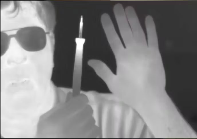
IRCameras has incorporated an SLS sensor from Qmagiq (Nashua, NH) into both a commercial, off-the-shelf science-grade IR camera and an OEM core configuration. This sensor operates over the spectral range of 3 to 11 μm, with some sensitivity out to 12 μm. Based on a digital readout integrated circuit (ROIC) from Santa Barbara Focalplane, the Qmagiq broadband SLS detector is a 640 × 512 format, 20-μm-pitch design that operates at up to 475 frames/s. With real-time frame averaging in the IRCameras’ imager-system electronics, noise-equivalent temperature differences (NETDs) of less than 8 mK are possible with real-time imagery displayed at 30 frames/s (see Fig. 2). The broadband response of the SLS sensor allows a single camera to address both MWIR and LWIR applications, where previously two separate systems were required.

Figure 2. A scene captured with an LWIR strainer layer superlattice (SLS) broadbad FPA with 640 x 512 format and using an LWIR optic shows one of the authors, Arn Adams, holding a hot soldering iron.
IRCameras has incorporated an SLS sensor from Qmagiq (Nashua, NH) into both a commercial, off-the-shelf science-grade IR camera and an OEM core configuration. This sensor operates over the spectral range of 3 to 11 μm, with some sensitivity out to 12 μm. Based on a digital readout integrated circuit (ROIC) from Santa Barbara Focalplane, the Qmagiq broadband SLS detector is a 640 × 512 format, 20-μm-pitch design that operates at up to 475 frames/s. With real-time frame averaging in the IRCameras’ imager-system electronics, noise-equivalent temperature differences (NETDs) of less than 8 mK are possible with real-time imagery displayed at 30 frames/s (see Fig. 2). The broadband response of the SLS sensor allows a single camera to address both MWIR and LWIR applications, where previously two separate systems were required.
Arn Adams is technical director and Elliott Rittenberg is vice president of sales and marketing at IRCameras LLC, Santa Barbara, CA; e-mail: elliott@ircameras.com; www.ircameras.com.
